
Laminated Busbar Design and Manufacturing for Low-Inductance Power Systems
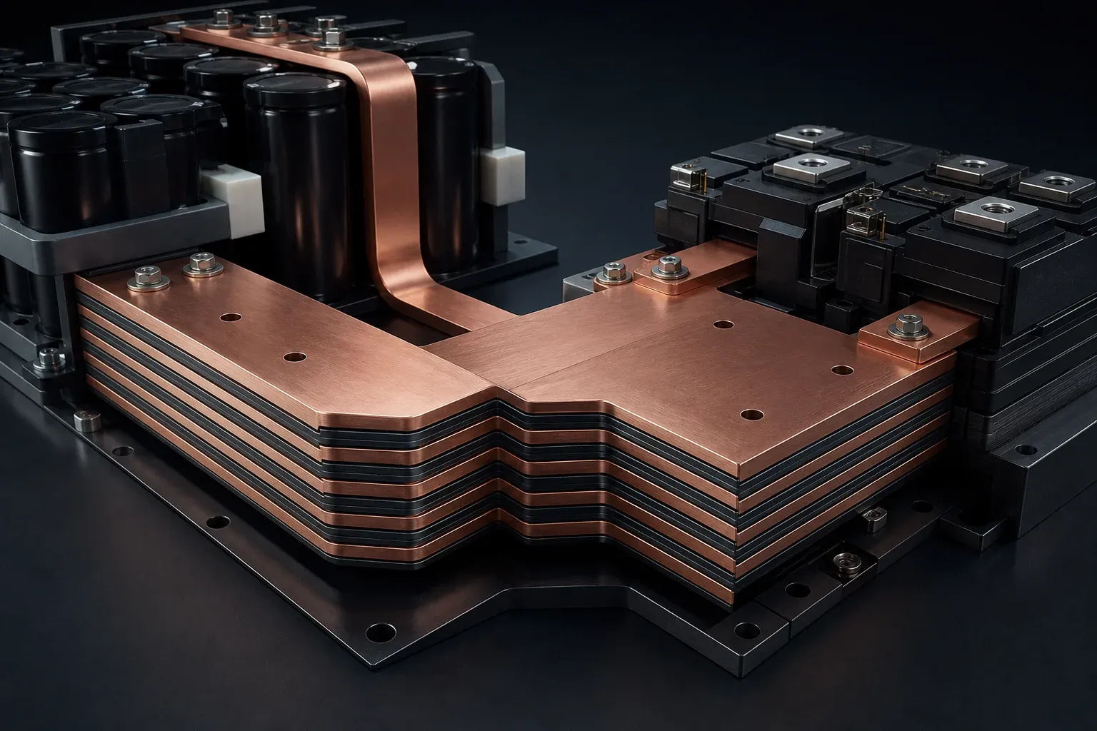
A laminated busbar is useful when it controls the current loop. Copper plates separated by dielectric film may look compact, but the switching path can still have excessive stray inductance if the positive and negative conductors separate at the terminals, take long routes to a capacitor, or create a large loop around a power module.
Design therefore begins with the electrical network and component interfaces, not with the external busbar outline. Manufacturing decisions—copper thickness, edge treatment, terminal machining, layer registration, adhesive, pressure, and cure—then have to preserve the intended geometry.
Define the Commutation Loop Before Drawing the Outline
Map the high-di/dt path through the DC-link capacitor, switching devices, and return conductor. Identify which section must have low inductance and which connections are outside that critical loop. Also capture voltage, current waveform, switching speed, allowable overshoot, thermal limits, component tolerances, and mechanical keep-out zones.
This prevents two common errors. The first is optimizing a flat central region while ignoring long terminal tabs. The second is using a generic inductance target without stating the frequency range, measurement method, or portion of the assembly included.
Research such as the Oak Ridge National Laboratory work on commutation-loop inductance in a 135 kW SiC EV inverter shows why estimation, minimization, and validation must be connected. Its geometry and results belong to that inverter; the transferable lesson is the method, not a universal number.
Use Overlap and Layer Spacing to Control Loop Area
When outgoing and return currents flow in closely spaced, overlapping conductors, their magnetic fields partially oppose and the enclosed loop area becomes smaller. Increasing useful overlap and reducing separation can therefore reduce stray inductance. The practical limits are set by dielectric requirements, manufacturing thickness, thermal behavior, terminals, and mechanical durability.
| Design variable | Expected direction | Main trade-off | How to verify |
|---|---|---|---|
| Greater positive/negative overlap | Usually lowers loop inductance | Larger component, capacitance and edge complexity | Field/circuit model plus measurement |
| Smaller conductor separation | Usually lowers loop inductance | Dielectric stress and manufacturing tolerance | Stack analysis and dielectric validation |
| Shorter terminal path | Reduces local loop contribution | Packaging and service access | Include terminals in model and test fixture |
| Wider current path | Can reduce resistance and current crowding | Size, material, uneven current sharing | Current-density and thermal analysis |
| Symmetric parallel connections | Can improve current sharing | More terminals and tolerance stack | Branch-current or thermal validation |
The 2024 review of laminated busbar design is a useful map of design approaches, but every cited result retains its own topology, frequency, materials, and test conditions.
Select Copper, Dielectric, Adhesive, and Edge Treatment as a Stack
The stack is a coupled system. Copper thickness affects resistance, heat spreading, stiffness, punching behavior, and the space available for dielectric layers. The dielectric material contributes electrical strength, temperature capability, thickness tolerance, flexibility, adhesion, and environmental ageing. The bonding process determines whether those properties survive lamination.
Edge design is especially important because conductors do not normally terminate at identical shapes everywhere. Insulation setback, sealed edges, local reinforcement, molded features, and mounting holes can create concentrated electrical or mechanical stress. The assembly drawing should define the exposed copper, dielectric extension, minimum edge geometry, and any areas that must remain free for contact.
Material names are not enough. Specify the supplier grade, thickness, condition, storage limits, and qualified process. A “polyimide” or “epoxy” description without a product and stack-up leaves the manufacturing team unable to reproduce the prototype.
Treat Terminations as Part of the Low-Inductance Design
Capacitor and semiconductor terminals often dominate an otherwise good layout. A wide overlapping pair of plates may separate into narrow tabs just before the device, creating current crowding and a larger local loop. Fastener access can also force unnecessary path length.
Review the following at each interface:
- positive and negative terminal spacing and overlap;
- bolt, pin, weld, or press-fit connection method;
- hole and slot tolerances relative to the component datum;
- contact-surface flatness and finish;
- current sharing between parallel terminals;
- assembly order and tool access;
- tolerance stack between the busbar, capacitor, module, and enclosure;
- strain transferred into ceramic or plastic component bodies.
The SAE study on integrated busbar design for a high-power SiC traction inverter is relevant application evidence, but its conclusions should remain tied to its inverter architecture.
Design for Copper Fabrication and Lamination
Each copper layer needs a stable datum and a process route for punching, profiling, forming, deburring, cleaning, and finishing. A CNC punching and shearing workstation may produce layer profiles and terminal features, but it does not perform the complete lamination process.
After copper fabrication, production must control:
- burr direction and edge condition;
- cleanliness before bonding;
- dielectric cut shape and registration;
- adhesive or bonding-film condition;
- stack alignment and tooling datums;
- lamination pressure, temperature, and time according to the qualified process;
- cure or cooling without warpage;
- trimming, sealing, and terminal exposure;
- final dimensions and electrical tests.
A change in copper supplier, dielectric lot, adhesive, cure cycle, or tool datum may affect both fit and electrical behavior. That is why prototype data should be tied to a controlled bill of materials and process revision.
Validate Electrical, Thermal, Dielectric, and Mechanical Performance
No single test proves the design. Inductance or switching behavior must be measured with a fixture and bandwidth appropriate to the application. Thermal validation must include conductor loss, joint loss, nearby heat sources, airflow, and the real duty cycle. Dielectric verification must reflect the voltage stress, edge construction, environment, and applicable standard. Mechanical inspection covers layer registration, warpage, terminal plane, mounting fit, and edge integrity.
For power-electronic switching, compare model and measurement rather than choosing whichever produces the lower number. Unexpected disagreement can reveal omitted terminal inductance, fixture effects, material assumptions, or current paths outside the model.
Complete a DFM Review Before Prototype Release
| Review area | Release question |
|---|---|
| Electrical path | Is the complete outgoing and return loop defined, including terminals? |
| Stack | Are every conductor, dielectric, adhesive, and finish grade controlled? |
| Geometry | Are datums, registration, cutbacks, edges, and terminal planes measurable? |
| Process | Can each layer be formed and deburred without damaging the intended stack? |
| Assembly | Can components be installed without forcing the busbar or loading fragile terminals? |
| Validation | Do simulation and tests use the same boundaries and controlled prototype? |
| Change control | Which material or process changes require engineering review or requalification? |
The resulting component can serve 800 V EV power electronics, utility-scale BESS, and emerging 800 VDC data center architectures. Those applications should share a DFM discipline, not a copied busbar geometry.
Frequently Asked Questions (FAQs)
How does a laminated busbar reduce stray inductance?
It can place outgoing and return-current conductors close together with substantial overlap, reducing the enclosed commutation-loop area. The result depends on the complete path, especially terminals and component connections, so lamination alone does not guarantee low inductance.
What is the difference between a laminated and a flexible busbar?
A laminated busbar is organized around layered conductors and dielectric material, often to control electromagnetic performance and packaging. A flexible busbar is organized around movement accommodation. Some products combine both characteristics, but the design inputs and validation priorities remain distinct.
Which dielectric materials are used in laminated busbars?
The choice depends on voltage stress, temperature, thickness, adhesion, flame and environmental requirements, edge construction, and the manufacturing process. Use the material supplier's current data and validate the complete stack rather than selecting by polymer name alone.
How is laminated busbar inductance validated?
Designers commonly combine field or circuit simulation with impedance, switching-waveform, or application-level measurements. The model and test fixture must include the terminals, capacitors, power modules, and current return path relevant to the real system.
Which manufacturing tolerances matter most at the terminals?
Hole or slot position, terminal plane, layer registration, cutback, flatness, and the relationship to the mating component datums are usually critical. The actual limits must come from the approved system drawing and assembly analysis.
DHCNC-BP-60 CNC Punching & Shearing Workstation
Discover details, parameters, standard dies packages, and factory quotes.